Welcome: Shenzhen Zhuolida Electronics Co.TD
Language:
 ∷
∷

∷
∷
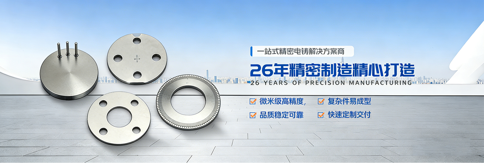
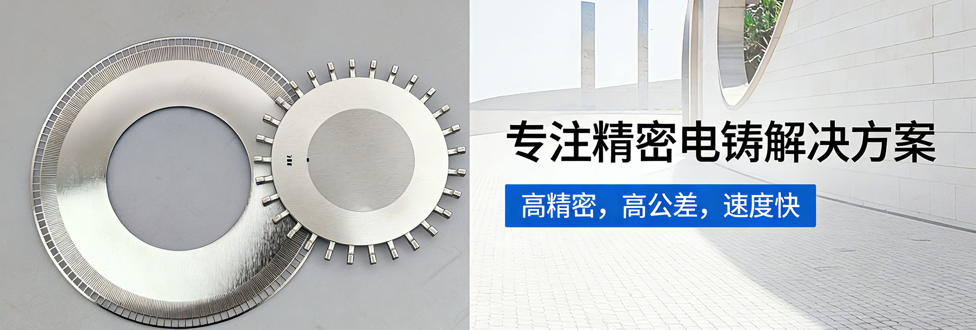
Professional technology and standardized management
12
 0755-2708-8292
Staying true to our founding mission in electroforming technology R&D, we explore new materials while adhering to scientific principles.
Delivering high-quality electroforming product solutions to customers worldwide

With 26 years of deep expertise in the electroforming field, we have established a comprehensive integrated system encompassing pr

The six professional technical certifications we offer are all built upon audit standards that strictly adhere to the ISO manageme

Leveraging extensive expertise in electroforming, we have successfully provided customized solutions for over 3,000 domestic clien
Deeply cultivating the path of electroforming technology innovation, rigorously selecting cutting-edge materials, and meticulously refining core processes.
Innovation-Driven / People-Centered / Customer-First
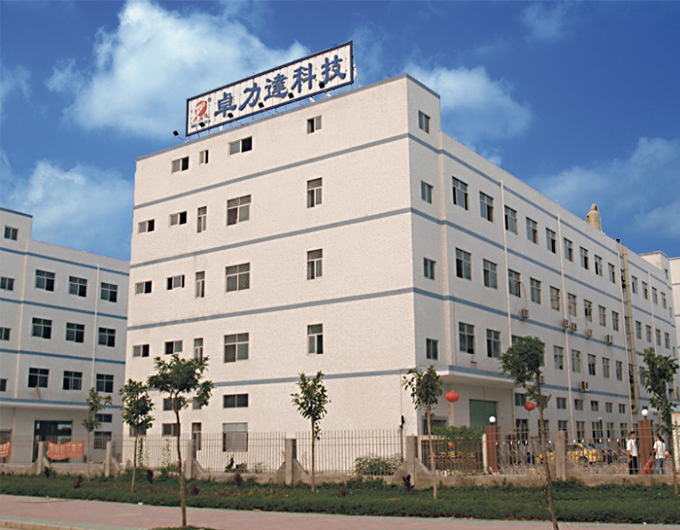
We have been transforming the ideas and visions projects.
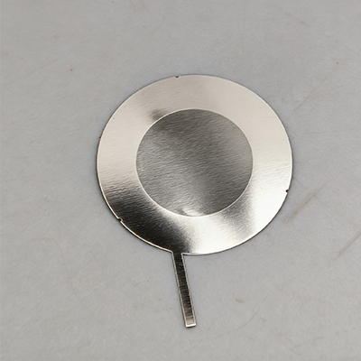
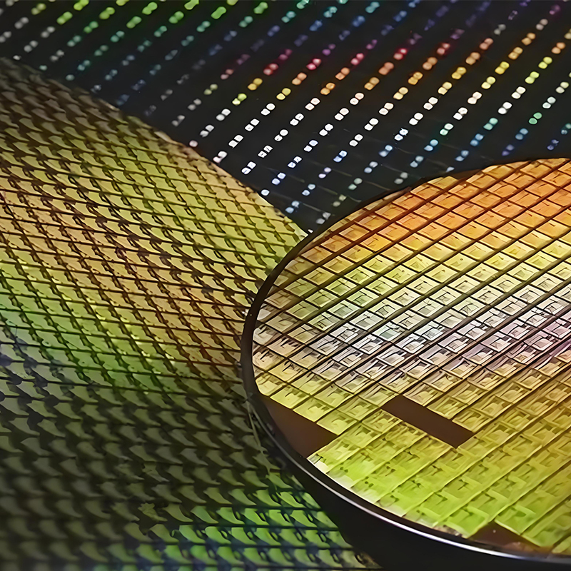
Zhuolida was established in 2000. Its core business encompasses multiple fields including high-end precision metal etching, SMT laser stencils, electroformed wafer stencils, precision electroformed components, electroplating surface treatment, semiconductor component cleaning, semiconductor machining, and semiconductor surface treatment. It is recognized as a National...
READ MOREStay tuned to Zhuolidata's development and stay ahead of the electroforming market trends.
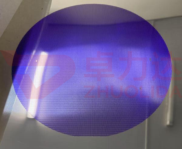
Core Factors Affecting Electroform
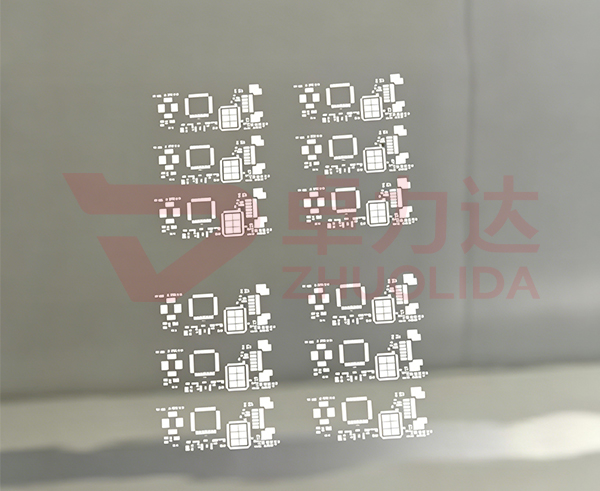
When calculating costs, Shenzhen Zhuolida Electroforming Manufacturing breaks down the expenses across multiple stages, including master pla
Analysis of Electroforming and Ele
A comparison of electroforming and electroplating is the foundation for selecting precision manufacturing processes. This is particularly tr
Process Requirements and Industria
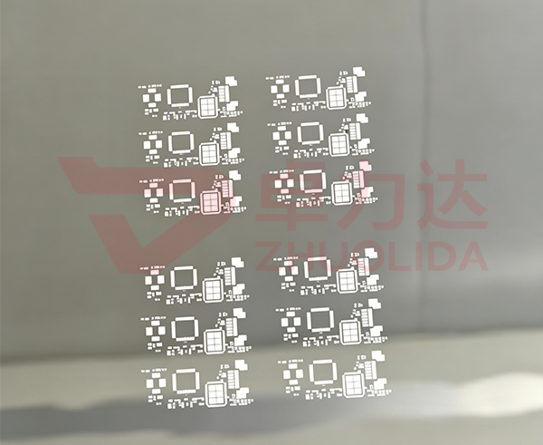
The stencil for IC carrier boards with uบอล packaging is manufactured using a one-step additive process via pulse electroforming with a nick
Actively expanding domestic and international markets, we have established long-term cooperative relationships with numerous renowned enterprises.




 Zhuolida