Welcome: Shenzhen Zhuolida Electronics Co.TD
Language:
 ∷
∷

∷
∷
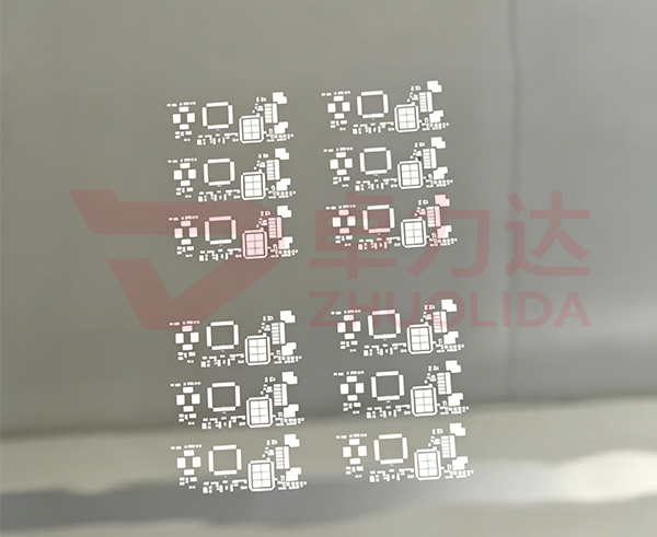
With the continuous miniaturization, high-density and ultra-thin upgrading of advanced semiconductor packaging processes, strict standards are imposed on the dimensional accuracy, hole wall smoothness and plate flatness of matching templates for wafer dicing, pre-dicing positioning and protective glue coating. Templates manufactured by traditional laser and etching processes usually suffer from stepped hole walls, stress deformation and inconsistent aperture sizes, which easily lead to wafer chipping, dicing offset and uneven glue coating, lowering chip yield. Semiconductor packaging wafer dicing templates are integrally formed by high-purity nickel electroforming additive manufacturing. Free of mechanical processing stress, they feature vertical and smooth openings and uniform array dimensions, compatible with 8-inch and 12-inch wafer dicing production, serving as core precision tooling for advanced packaging production lines. Electroforming processing of packaging wafer dicing templates adopts a standardized Class 100 dust-free constant temperature production line with optimized deposition parameters for ultra-thin and dense micropore templates, supporting small-batch R&D sampling and mass delivery. Electroforming processing companies of packaging wafer dicing templates continuously upgrade pulse electroforming technologies, micropore compensation schemes and post-cleaning processes to solve industrial pain points including uneven forming of dense micropores and easy deformation after long-term use, providing stable supporting services for various semiconductor packaging processes.
Semiconductor packaging wafer dicing templates take high-purity nickel as the forming substrate, with thickness ranging from 0.03mm to 0.15mm. The density of micropore arrays and coaxiality of positioning holes directly affect wafer dicing accuracy. The complete electroforming processing of packaging wafer dicing templates includes nine standard procedures: high-precision photolithography master mold fabrication, ultra-clean substrate activation, uniform conductive film deposition, pulsed layered nickel electroforming, low-temperature constant temperature stress relief, non-destructive demolding, micropore shaping and passivation, full-range precision inspection and anti-static dust-free vacuum packaging. During the whole production, current density, solution temperature and circulation flow rate are adjusted in real time to accurately control nickel grain growth, avoiding processing defects such as elliptical micropores, plate warpage, uneven thickness and rough inner walls. With dense structure and balanced toughness, semiconductor packaging wafer dicing templates are resistant to relaxation and deformation under repeated glue coating and clamping, suitable for 7脳24-hour continuous operation on packaging production lines. Electroforming processing companies of packaging wafer dicing templates build differentiated process parameter libraries for memory chips, logic chips and power chips to realize standardized production of multiple specifications.
High-precision master mold fabrication and ultra-clean pretreatment are core pre-processes ensuring forming accuracy in electroforming processing of packaging wafer dicing templates. All wafer positioning micropores, dicing clearance grooves and outer frame positioning holes are replicated from high-precision negative master molds, and dimensional deviations of master molds will be passed on to finished templates. Exclusive master molds are designed according to wafer layouts and dicing street dimensions before production, and micro-nano photolithography and precision grinding shaping are adopted to eliminate hidden dangers such as hole position offset and groove deformation. Master molds are made of low-expansion and high-flatness special substrates, which go through multi-stage degreasing, circulating ultrapure water rinsing and plasma activation purification to thoroughly remove surface dust, oil stains and oxide films for uniform conductive film adhesion. Micron-level dimensional compensation is preset for ultra-high-density micropore areas to offset tiny dimensional errors caused by lateral erosion during electroforming. Relying on high-precision master mold replication, semiconductor packaging wafer dicing templates stably achieve micron-level array tolerances and meet zero-defect standards for high-end wafer packaging. Electroforming processing companies of packaging wafer dicing templates refine regular maintenance and re-inspection specifications for master molds to reduce the defective rate of mass products from the source.
Pulsed layered electroforming deposition is the core forming link of electroforming processing of packaging wafer dicing templates. Pre-treated master molds are sent to a closed ultra-clean workstation for uniform dense conductive film coating to avoid local deposition fracture and incomplete micropores. The master molds are placed in semiconductor-specific low-stress electroforming tanks equipped with high-precision pulse current control systems for layered intermittent nickel deposition. The layered deposition mode continuously releases forming stress, producing semiconductor packaging wafer dicing templates with flat surfaces and micropores free of steps and burrs without secondary hole polishing. Free of mechanical extrusion and high-temperature thermal damage, the whole forming process leaves no hidden stress on finished products, so aperture drift will not occur under long-term repeated clamping. Electroforming processing companies of packaging wafer dicing templates continuously optimize the filtering and circulation system of electroforming solution to reduce micropore blockage caused by metal particle adhesion and greatly extend the service life of templates.
Stress relief, non-destructive demolding and clean post-treatment directly determine the stability of finished products from electroforming processing of packaging wafer dicing templates. After electroforming reaches the preset thickness, semi-finished products are placed in a low-temperature constant temperature chamber for long-term stress relief to completely eliminate subtle internal stress generated during metal deposition and enhance deformation resistance. Flexible demolding media are used to separate templates from master molds smoothly, avoiding micropore stretching and plate wrinkles caused by forced pulling. Post-demolding procedures include multi-stage ultrapure water cleaning, micropore dredging and anti-oxidation passivation. The thin and dense passivation film will not affect template positioning accuracy while resisting corrosion by acid-base mist in packaging workshops. All finished products pass comprehensive tests via image measuring instruments, flatness testers and aperture uniformity testers, with unqualified products sorted out and scrapped. Qualified products are vacuum packaged in a Class 100 dust-free environment. After multi-layer cleaning, semiconductor packaging wafer dicing templates contain no precipitated impurities and will not contaminate wafer surface glue and chip circuits. Electroforming processing companies of packaging wafer dicing templates implement piece-by-piece inspection control to guarantee all indicators of delivered templates meet standards.
In terms of practical packaging industry application, semiconductor packaging wafer dicing templates are widely used in three mainstream scenarios: memory wafer packaging, automotive power chip packaging and high-end logic chip packaging, featuring high precision, low stress and high cleanliness. Electroforming processing of packaging wafer dicing templates can customize micropore arrays according to different wafer sizes and dicing street pitches, meeting the demands of new product R&D sampling and mass production of mature chips. Electroforming processing companies of packaging wafer dicing templates adjust post-treatment procedures based on the working conditions of various packaging production lines to adapt to production workshops with high temperature and high cleanliness requirements.
For memory wafer packaging, semiconductor packaging wafer dicing templates deliver highly consistent micropore arrays for uniform protective glue coating, effectively lowering the probability of wafer chipping and chip damage during dicing. Electroforming processing of packaging wafer dicing templates strictly controls hole wall verticality to reduce residual glue adhesion. Electroforming processing companies of packaging wafer dicing templates optimize micropore smoothness processes to match the precise dicing demands of high-density memory wafers.
For automotive power chip packaging, the low-stress structure of semiconductor packaging wafer dicing templates ensures stable positioning hole coaxiality under long-term high-frequency use without offset after repeated clamping. Electroforming processing of packaging wafer dicing templates thickens the passivation protective layer to resist corrosion by volatile chemicals in workshops. Electroforming processing companies of packaging wafer dicing templates strengthen plate flatness processes to satisfy high-reliability packaging standards for automotive-grade chips.
For high-end logic chip packaging, the ultra-thin thickness of semiconductor packaging wafer dicing templates adapts to ultra-narrow dicing streets, with micro clearance grooves integrally formed without interfering with cutter operation. Electroforming processing of packaging wafer dicing templates adopts full dust-free production without metal debris contaminating precision chip circuits. Electroforming processing companies of packaging wafer dicing templates tightly control overall thickness tolerances to meet precise dicing processes for micro logic chips.
In conclusion, semiconductor packaging wafer dicing templates break the limitations of traditional processing templates including insufficient precision, easy deformation and poor cleanliness, acting as indispensable precision tooling for modern wafer dicing and packaging. Relying on standardized dust-free, constant temperature and low-stress electroforming processes, electroforming processing of packaging wafer dicing templates realizes stable mass production of high-precision dicing templates. Electroforming processing companies of packaging wafer dicing templates continuously delve into semiconductor-specific electroforming technologies and optimize micropore forming and clean treatment techniques, providing reliable precision supporting solutions for the high-quality development of advanced packaging industries covering memory, automotive and logic chips.
Contact:赖先生
Phone:+86 18938693450
Tel:0755-2708-8292
Email:yw9@zldsmt.com
Add:深圳市宝安区福永镇新和村福园一路华发工业园A3栋
 Zhuolida